Features
·General Porting Considerations
·Memories
·System Clock and Clock Options
·System Control and Reset
·Registers
·Interrupts
·Timer/Counters
·USI – Universal Serial Interface
·Analogue-to-Digital Converter
·I/O Ports
·Memory Programming
·Electrical Characteristics
1 Introduction
This application note is a guide to assist users of ATtiny26 in converting existing designs to ATtiny261A. The document will also assist ATtiny26 users to migrate to the ATtiny461A and ATtiny861A devices, which are members of the same family as the ATtiny261A, offering larger memories.
In addition to the differences described in this document, the electrical characteristics of the devices are different. Some of these differences are outlined in this document and some are not. Please check the latest data sheets for detailed information.
Improvements or added features in ATtiny261A that are not in conflict with those in ATtiny26 are not listed in this document.
Note: This application note serves as a guide to ease migration. For complete device details, always refer to the most recent version of the ATtiny261A/461A/861A data sheet.
2 General Porting Considerations
Between the devices described in this application note, some registers and register bits have changed name but note that they preserve the same functionality. They are all listed later in this document. To make the porting process as easy as possible, always refer to registers and bit positions using their defined names. Avoid using absolute addresses and values. In most cases, the register and bit names are unchanged from device to device. When you are porting a design, it is more convenient to include the correct definition file for the new device, rather than manually changing all your addresses and bit values. It is also considered good programming practice to use named references instead of absolute values. Some examples are shown below.
2.1 Current Consumption
Active and Idle mode current consumption of the device has been reduced significantly. The tables below present typical current consumption figures at room temperature. All values are taken from device datasheets, unless otherwise noted.
PORTB |= (1<< PORTB3); // Set pin 3 on port B high
DDRB &= ~(1<< PORTB3); // Set pin 3 on port B as input
// Configure USI
USICR = (1<< USISIE)|(0<< USIOIE)|(1<< USIWM1)|(0<< USIWM0)|
(1<< USICS1)|(0<< USICS0)|(0<< USICLK)|(0<< USITC);
To avoid conflicts with added features and register functionality, never access registers that are marked as reserved. Reserved bits should always be written to zero if accessed. This ensures forward compatibility, and added features will stay in their default states when unused.
3 Memories
ATtiny26 and ATtiny261A have the same amount of volatile and non-volatile memory. ATtiny461A and ATtiny861A have more SRAM, Flash and EEPROM than ATtiny26. Applications that rely on the size of memory may therefore misbehave when memory size is increased. For example, this may be the case with wrap-around indexing of EEPROM.
3.1 Stack
The ATtiny26 stack pointer is implemented as an 8-bit register in the I/O space. In ATtiny261A the stack pointer is also realized as one 8-bit register, but in ATtiny461A and ATtiny861A the amount of data memory exceeds the 8-bit address range and the stack pointer has been realized as two 8-bit registers. See table below.

See ATtiny261A/461A/861A data sheet for information on how to access stack pointer registers.
3.2 EEPROM
EEPROM write access times depend on the frequency of the internal RC oscillator. In ATtiny261A/461A/861A the access times are shorter than in ATtiny26.
ATtiny261A is part of a pin and functionally compatible subfamily of tinyAVR(R), where the size of EEPROM ranges from 128 to 512 bytes. This means more than eight data bits are required for memory addressing and, therefore, the EEPROM address register has been expanded from one 8-bit register (EEAR in ATtiny26) to two (EEARL and EEARH in ATtiny261A, ATtiny461A and ATtiny861A). Since the initial values of the registers are undefined it is important to always write both registers even when accessing only the bottom section of the EEPROM.
4 System Clock and Clock Optio
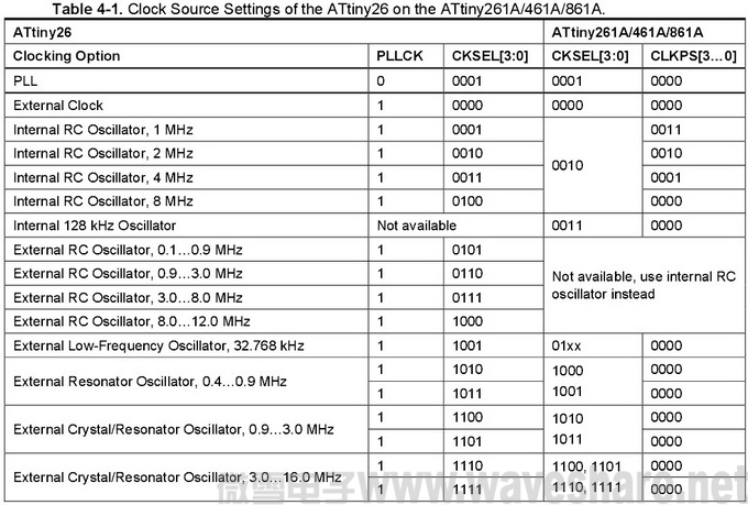
ATtiny261A/461A/861A has a more advanced clock system than ATtiny26. In ATtiny261A/461A/861A there is a system clock prescaler and three internal clock sources.
4.1 Clock Sources
Clock source options are set differently in ATtiny261A/461A/861A. See table below how to set the ATtiny26 settings on the ATtiny261A/461A/861A.
4.2 High Frequency PLL Clock
When using the internal PLL as a clock source, ATtiny261A/461A/861A applies a longer start-up delay than ATtiny26 after a power-on reset and power-down wakeup. This is to ensure stable and glitch-free operation.
5 System Control and Reset
ATtiny261A/461A/861A has more fuse bits than ATtiny26. In addition, some fuse bits have a different functionality.
5.1 Brown-Out Detection (BOD)
Both ATtiny26 and ATtiny261A/461A/861A have programmable Brown-Out Detection levels. The programming method and levels are not entirely the same. See table below.

5.2 Start-up Times & Brown-out Detection
Due to electrical differences between ATtiny26 and ATtiny261A/461A/861A there may be minor dissimilarities in start-up times. Please see device data sheets for more detailed information.
5.3 Power-On Reset
The table below summarizes the differences between the reset circuitry of ATtiny26 and that of ATtiny261A/461A/861A. Please see device data sheets for more detailed information.

5.4 Watchdog Timer
The ATtiny261A/461A/861A includes an enhanced Watchdog Timer (WDT), compared to the watchdog timer used in ATtiny26. At 5V operating voltage the WDT will behave similar on ATtiny26 and ATtiny261A/461A/861A. At lower voltages the watchdog timeout interval may differ. Please see data sheet for characteristic data on watchdog oscillator frequency. If the WDT is not used, it is still recommended to disable it initially in the application code to clear unintentional WDT enabled events.
6 Registers
6.1 Renamed Registers
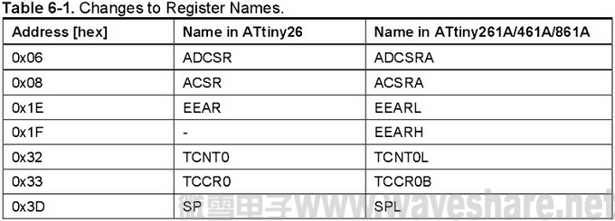
The below tables list the registers which have been renamed but still exist at the same physical address and have maintained their functionality. It is only required to update the register name in the application.
6.2 Renamed Bits
The below table lists the bits that have been renamed, but still exist in the same register and in the same register location.

p>
6.3 Removed BitsThe below table lists register bits, which have been removed and have no close replacements.

p>
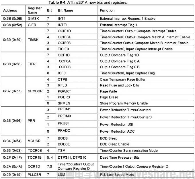
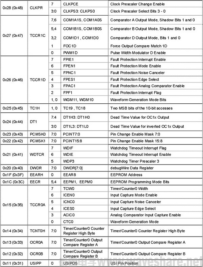
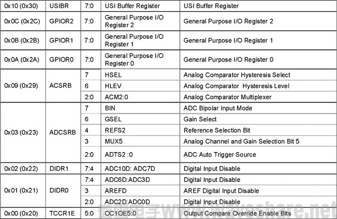
6.4 New Registers and Bits The new registers and bits for ATtiny261A/461A/861A can be seen in the following table. See the data sheet for the full description.
7 Interrupts
7.1 Interrupt Vectors
ATtiny261A/461A/861A has more interrupt vectors than ATtiny26, but all ATtiny26 vectors exist in identical locations on ATtiny261A/461A/861A. Programs can still use the end of ATtiny26 interrupt vector table as a starting address on ATtiny261A/461A/861A, provided that ATtiny261A/461A/861A specific interrupts are not enabled. Additional interrupt vectors can be seen at the table below.

7.2 Pin Change Interrupt
Pin change interrupts are automatically disabled on ATtiny26 if an alternative function has been enabled for the given pin. In ATtiny261A/461A/861A this is not the case, where alternative pin functions and pin change interrupts may be concurrently enabled for the same pin. Pin change interrupts for a given pin in ATtiny261A/461A/861A are masked and unmasked using Pin Change Mask Register A (PCMSKA) and Pin Change Mask Register B (PCMSKB).
7.2.1 Source Pins and Masking
ATtiny261A/461A/861A extends pin change interrupts to cover all I/O pins, while ATtiny26 only includes pins PA3, PA6…7 and PB0…7. Also, ATtiny261A/461A/861A allows individual masking of pin change interrupt sources via registers PCMSK0 and PCMSK1 (a feature not found in ATtiny26) but the default setting is to enable only those sources that are common for both ATtiny26 and ATtiny261A/461A/861A.
8 Timer/Counters
8.1 Timer/Counter1
In ATtiny261A/461A/861A the synchronization registers are not bypassed as in ATtiny26. This means a synchronization delay of 1.5 clock cycles is present in both asynchronous and synchronous modes.
8.1.1 Bit CTC1 of Register TCCR1B
Bit CTC1 of register TCCR1B has been replaced by PWM1X on ATtiny261A/461A/861A. Please note that these bits have a different functionality and that this must be considered during migration.
8.1.2 Register OCR1C
Register OCR1C is now always the TOP value for the timer/counter and the register is always reset (cleared to zero) after reaching the TOP value. The lowest allowed TOP value is 3. If register OCR1C is loaded with a value lower than 3 it will be forced to the value 3. Also note that after a reset the OCR1C register is loaded with the timer/counter MAX value, which means that the default TOP value is 0x3FF.
8.1.3 PWM Mode
When writing to register OCR1C on ATtiny261A/461A/861A the data is buffered and the register updated only when OCR1C has reached the TOP value. In ATtiny26 writing to OCR1C is immediate.
9 USI – Universal Serial Interface
The ATtiny261A/461A/861A uses an enhanced version of the Universal Serial Interface, as compared to the ATtiny26.
9.1 Clock Sources
The USI clock can be selected from three different sources, two of which are common for ATtiny26 and ATtiny261A/461A/861A. The third clock source option (USICS[2:0] = 01X) in ATtiny26 is Timer/Counter0 Overflow, but in ATtiny261A/461A/861A it has been replaced by Timer/Counter0 Compare Match. Similar functionality can be achieved but it may be necessary to update any parts of firmware that refer to Timer/Counter0 overflow flags and interrupts.
10 Analogue-to-Digital Converter
The Analogue-to-Digital Converter (ADC) has been enhanced and in ATtiny261A/461A/861A includes more features. ATtiny261A/461A/861A is a 1.8V device and the default internal voltage reference is therefore set to 1.1V.
10.1 Voltage Reference Selection
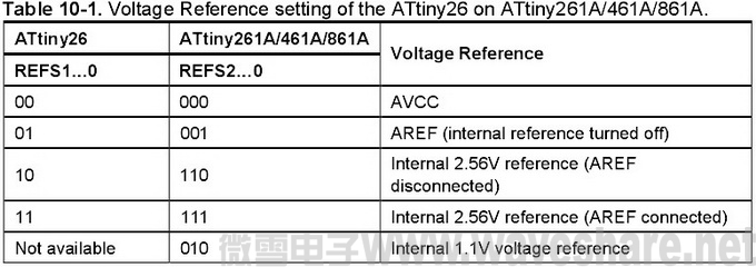
Voltage reference source is selected using bits REFS2…0, located in registers ADMUX (ADC Multiplexer Selection) and ADCSRB (ADC Control and Status Register B). ATtiny26 only includes bits REFS1…0. The table below shows how to update reference selection bits to maintain functionality.
11 I/O Ports
Test limits for port drive strength are lower on ATtiny261A/461A/861A. This means ATtiny261A/461A/861A ports are rated for a lower current than ATtiny26. Port driver characteristics are outlined in the table below.

12 Memory Programming
Some modifications regarding the programming of fuse and calibration bytes must be taken into account. Also, the functionality of the calibration byte has been changed.
12.1 Fuse Bits
The number of fuse bits has been increased and fuse b bytes in ATtiny261A/461A/861A. Read and write algor proper fuse programming. The functionality of the following fuse bits has changed: ·The BODLEVEL fuse bit of ATtiny26 has been expanded to three fuse bits (BODLEVEL2…0) on ATtiny261A/461A/861A.
·The BODEN fuse bit functionality of ATtiny26 has been integrated into BODLEVEL2…0 fuse bits of ATtiny261A/461A/861A.
·The PLLCK and CKOPT fuse bit functionality of ATtiny26 has been integrated into CKSEL3…0 fuse bits of ATtiny261A/461A/861A.
·Clock prescaler functionality of CKSEL fuses has been removed, since ATtiny261A/461A/861A has a software configurable clock prescaler.
12.2 Signature Bytes
Signature bytes reside in a separate address space and can only be read external to the device. Therefore, this notion only applies to programmers, et al, and not to the actual program being migrated. Signature bytes have been updated as illustrated in the table below.

12.3 Calibration Byte
ATtiny26 has four calibration bytes for the 1MHz, 2MHz, 4MHz and 8MHz operation of the internal RC oscillator. ATtiny261A/461A/861A only has one calibration byte for the internal RC oscillator.
13 Electrical Characteristics
ATtiny261A/461A/861A is manufactured using a different process than ATtiny26 and electrical characteristics will therefore differ between these devices. For detailed information, refer to the most recent version of the device data sheets.